Guest Lecture »Atomic Diffusion Bonding of Wafers«
In a presentation of Prof. Takehito Shimatsu – partner and visiting lecturer of Waferbond ’22 conference – latest research on wafer bonding will be discussed.
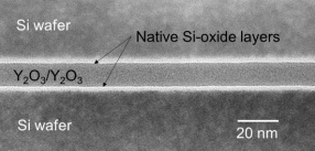
Atomic diffusion bonding (ADB) of wafers is a promising process to achieve roomtemperature wafer bonding. In standard ADB, thin metal films are fabricated on two flat wafer surfaces using sputter deposition, followed by bonding of the two films on the wafers in vacuum. Recently we demonstrated ADB of wafers at room temperature using oxide films [1]. No interface corresponding to the original film surface was observed (Figure 1), indicating high performance of bonding using Y2O3 films. Incident light can pass through transparent wafers bonded with oxide films without reduction in intensity (Figure 2). Moreover, the bonded films show a good electrical insulation. Any mirror-polished wafer can be bonded using oxide films. These properties are useful to produce new optical or electrical devices. We present the technical potential and current status of ADB using oxide films.
[1] T. Shimatsu, H. Yoshida, M. Uomoto, T. Saito, T. Moriwaki, N. Kato, Y. Miyamoto, and
K. Miyamoto, Proc. 7th Int. Workshop on LTB-3D, 2021, p. 51.

Lecturer Prof. Shimatsu-san is leading scientist in the field of wafer bonding at the Frontier Research Institute for Interdisciplinary Sciences at Tohoku University of Japan. Prof. Shimatsu is engaged in various organizations like the Japan Institute of Electronics Packaging, IEEE, the Magnetics Society, the Magnetics Society of Japan and the Japan Institute of Metals and Materials.
Attending the lecture is free of charge, industry partners, scientists and engineers of the photonics region of Jena are kindly invited.
Veranstaltungsform
Veranstaltungsort
Ernst-Abbe-Hochschule Jena | Haus 5 | HS 5
Carl-Zeiss-Promenade 2
07745 Jena
Deutschland
Kontakt
Ernst Abbe Hochschule Jena
Ronny Gerbach
03641 205–362
ed.anej-hae@hcabreg.ynnor
https://www.eah-jena.de/
Diese Veranstaltung buchen
Buchungen sind für diese Veranstaltung nicht mehr möglich.